We've just updated MediaWiki and its underlying software. If anything doesn't look or work quite right, please mention it to us. --RanAS
Work RAM: Difference between revisions
From SnesLab
(added size in bytes) |
(no more underscore) |
||
| Line 3: | Line 3: | ||
Even though WRAM has both [[Address Bus A]] and [[Address Bus B]] connected to it, the chip can only pay attention to one at a time, so WRAM-to-WRAM [[DMA]] isn't possible. | Even though WRAM has both [[Address Bus A]] and [[Address Bus B]] connected to it, the chip can only pay attention to one at a time, so WRAM-to-WRAM [[DMA]] isn't possible. | ||
WRAM is left intact by | WRAM is left intact by a [[Reset]]. [2] | ||
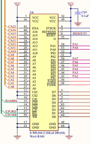
[[File:wram schematic.png|thumb|The WRAM chip is straddling regions C1 and D1 in the jwdonal schematic]] | [[File:wram schematic.png|thumb|The WRAM chip is straddling regions C1 and D1 in the jwdonal schematic]] | ||
Revision as of 06:34, 6 July 2023
WRAM (Work RAM) serves as the SNES' main memory. It is 128K x 8 bits (131,072 bytes) in size. It has part number 21326. [3]
Even though WRAM has both Address Bus A and Address Bus B connected to it, the chip can only pay attention to one at a time, so WRAM-to-WRAM DMA isn't possible.
WRAM is left intact by a Reset. [2]
References
- [1] https://problemkaputt.de/fullsnes.htm#snesmemoryworkramaccess
- [2] https://problemkaputt.de/fullsnes.htm#snescontrollersotherinputs
- page 1 of Book II, "Super NES Parts List" in the official Nintendo development manual
- https://archive.org/details/SNESDevManual/book1/page/n97

