We've just updated MediaWiki and its underlying software. If anything doesn't look or work quite right, please mention it to us. --RanAS
Front Panel Daughterboard: Difference between revisions
From SnesLab
(note about pins named after raw register addresses) |
(added alternate name) |
||
| Line 1: | Line 1: | ||
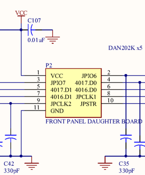
[[File:Front Panel Daughterboard schematic.png|thumb|The Front Panel Daughterboard is located in region A2 of the jwdonal schematic]] | [[File:Front Panel Daughterboard schematic.png|thumb|The Front Panel Daughterboard is located in region A2 of the jwdonal schematic]] | ||
The '''Front Panel Daughterboard''' is situated perpendicular to the SNES motherboard. It contains the two controller ports and the red power indicator LED. In the jwdonal schematic, pins 4, 6, 5, and 7 are named after '''JOYA''' and '''JOYB''', the [[fullsnes]] common names for the read-only joypad input registers A & B, who's addresses are '''4016h''' and '''4017h'''. | The '''Front Panel Daughterboard''' (known as the "'''Front Connector Unit''' in the official Nintendo documentation [1] ) is situated perpendicular to the SNES motherboard. It contains the two controller ports and the red power indicator LED. In the jwdonal schematic, pins 4, 6, 5, and 7 are named after '''JOYA''' and '''JOYB''', the [[fullsnes]] common names for the read-only joypad input registers A & B, who's addresses are '''4016h''' and '''4017h'''. | ||
=== References === | === References === | ||
* [1] Figure 2-22-1, "Super NES Functional Block Diagram" on page 2-22-2 of Book I: https://archive.org/details/SNESDevManual/book1/page/n97 | |||
* http://problemkaputt.de/fullsnes.htm#snescontrollersioportsmanualreading | * http://problemkaputt.de/fullsnes.htm#snescontrollersioportsmanualreading | ||
[[Category:SNES Hardware]] | [[Category:SNES Hardware]] | ||
Revision as of 06:16, 14 May 2023
The Front Panel Daughterboard (known as the "Front Connector Unit in the official Nintendo documentation [1] ) is situated perpendicular to the SNES motherboard. It contains the two controller ports and the red power indicator LED. In the jwdonal schematic, pins 4, 6, 5, and 7 are named after JOYA and JOYB, the fullsnes common names for the read-only joypad input registers A & B, who's addresses are 4016h and 4017h.
References
- [1] Figure 2-22-1, "Super NES Functional Block Diagram" on page 2-22-2 of Book I: https://archive.org/details/SNESDevManual/book1/page/n97
- http://problemkaputt.de/fullsnes.htm#snescontrollersioportsmanualreading


