We've just updated MediaWiki and its underlying software. If anything doesn't look or work quite right, please mention it to us. --RanAS
Checking Integrated Circuit: Difference between revisions
From SnesLab
(block diagram is on next page) |
(hid archive link) |
||
| Line 8: | Line 8: | ||
* https://snescentral.com/chips.php?chiptype=CIC | * https://snescentral.com/chips.php?chiptype=CIC | ||
* https://problemkaputt.de/fullsnes.htm#snescartridgeciclockoutchip | * https://problemkaputt.de/fullsnes.htm#snescartridgeciclockoutchip | ||
* [3] https://archive.org/details/SNESDevManual/book1/page/n98 | * [3] [https://archive.org/details/SNESDevManual/book1/page/n98 Page 2-22-2 of Book I] of the official Super Nintendo development manual | ||
[[Category:SNES Hardware]] | [[Category:SNES Hardware]] | ||
[[Category:Integrated Circuits]] | [[Category:Integrated Circuits]] | ||
Revision as of 16:06, 8 July 2023
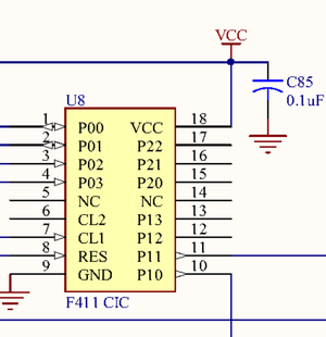
There are two CIC chips: one on the SNES Motherboard and one in the Game Pak. When the power is on, they are sending data streams to each other. If something goes wrong, the CIC in the Control Deck resets the console.
The CIC in the Control Deck has a 4.00 MHz clock, which also clocks the CIC in the Game Pak. [3]
External Links
- https://snescentral.com/chips.php?chiptype=CIC
- https://problemkaputt.de/fullsnes.htm#snescartridgeciclockoutchip
- [3] Page 2-22-2 of Book I of the official Super Nintendo development manual


