We've just updated MediaWiki and its underlying software. If anything doesn't look or work quite right, please mention it to us. --RanAS
VRAM: Difference between revisions
From SnesLab
(names of chips) |
(chips A & B named in schematic) |
||
| Line 5: | Line 5: | ||
The two chips can be referred to as "A" and "B", after the lines of the [[VRAM Data Bus]] VDA0~7 and VDB0~7. | The two chips can be referred to as "A" and "B", after the lines of the [[VRAM Data Bus]] VDA0~7 and VDB0~7. | ||
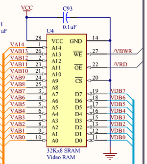
[[File:vram chip.png|thumb| | [[File:vram chip.png|thumb|VRAM chip B in region B2 of the jwdonal schematic (directly above chip A)]] | ||
[[Category:SNES Hardware]] | [[Category:SNES Hardware]] | ||
[[Category:Integrated Circuits]] | [[Category:Integrated Circuits]] | ||
[[Category:Video]] | [[Category:Video]] | ||
Revision as of 08:10, 25 May 2023
There are two VRAM chips on the SNES motheboard, both connected to S-PPU1.
One chip holds the low bytes of the 16-bit words, the other chip holds the high bytes.
The two chips can be referred to as "A" and "B", after the lines of the VRAM Data Bus VDA0~7 and VDB0~7.


