VRAM
From SnesLab

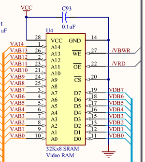
VRAM chip B in region B2 of the jwdonal schematic (directly north of chip A)
There are two VRAM chips on the SNES motherboard, both connected to S-PPU1. They are both SRAM and each 32K x 8 bit (32,768 bytes) in size, for a total of 65,536 bytes (one bank).
VRAM is word (not byte) addressed, with one chip holding the low bytes of the 16-bit words, the other chip holds the high bytes.
The two chips can be referred to as "A" and "B", after the lines of the VRAM Data Bus VDA0~7 and VDB0~7.
VRAM is not connected to Address Bus A, so the 5A22 must access it through I/O ports.
See Also
References
- Appendix A-1 of the official Super Nintendo development manual
- paragraph 22.4 on page 2-22-1 of Book I, lbid.

