We've just updated MediaWiki and its underlying software. If anything doesn't look or work quite right, please mention it to us. --RanAS
Front Panel Daughterboard: Difference between revisions
From SnesLab
(→References: hid archive URL) |
(→References: removed duplicate page number) |
||
| Line 5: | Line 5: | ||
=== References === | === References === | ||
* [1] Figure 2-22-1, "Super NES Functional Block Diagram" on | * [1] Figure 2-22-1, "Super NES Functional Block Diagram" on [https://archive.org/details/SNESDevManual/book1/page/n97 page 2-22-2 of Book I] of the official Super Nintendo development manual | ||
* http://problemkaputt.de/fullsnes.htm#snescontrollersioportsmanualreading | * http://problemkaputt.de/fullsnes.htm#snescontrollersioportsmanualreading | ||
[[Category:SNES Hardware]] | [[Category:SNES Hardware]] | ||
Revision as of 16:44, 8 July 2023

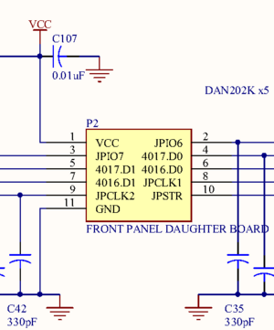
The Front Panel Daughterboard is located in region A2 of the jwdonal schematic
The Front Panel Daughterboard (known as the "Front Connector Unit in the official Nintendo documentation [1] ) is situated perpendicular to the SNES motherboard. It contains the two controller ports and the red power indicator LED. In the jwdonal schematic, pins 4, 6, 5, and 7 are named after JOYA and JOYB, the fullsnes common names for the read-only joypad input registers A & B, who's addresses are 4016h and 4017h.
References
- [1] Figure 2-22-1, "Super NES Functional Block Diagram" on page 2-22-2 of Book I of the official Super Nintendo development manual
- http://problemkaputt.de/fullsnes.htm#snescontrollersioportsmanualreading

