We've just updated MediaWiki and its underlying software. If anything doesn't look or work quite right, please mention it to us. --RanAS
HCU04: Difference between revisions
From SnesLab
(unconnected pins category) |
(linkify jwdonal schematic) |
||
| Line 4: | Line 4: | ||
* '''U9B''' outputs CL1 to the [[CIC]] | * '''U9B''' outputs CL1 to the [[CIC]] | ||
[[File:u9a%26b_schematic.png|thumb|U9A and U9B in region D2 of the jwdonal schematic]] | [[File:u9a%26b_schematic.png|thumb|U9A and U9B in region D2 of the [[jwdonal schematic]]]] | ||
The next two inverters help generate [[XIN]]: | The next two inverters help generate [[XIN]]: | ||
Revision as of 16:10, 8 July 2023
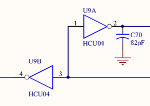
The HCU04 is a hex inverter. The first two inverters take SCLK from pin 41 of S-DSP as input:
- U9A outputs CIC3 to the Cartridge Slot
- U9B outputs CL1 to the CIC

U9A and U9B in region D2 of the jwdonal schematic
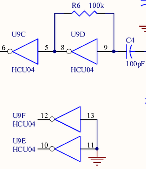
The next two inverters help generate XIN:
- U9C appears to undo the inversion that U9C did, and sends the output to R5, which eventually becomes XIN after passing by the pull-down R4
- U9D is in parallel with R6, receiving its input from C4 and outputting to U9C
The last two inverters take ground as input and their outputs are not connected:
- U9E
- U9F

