We've just updated MediaWiki and its underlying software. If anything doesn't look or work quite right, please mention it to us. --RanAS
Audio RAM: Difference between revisions
From SnesLab
(ARAM is one bank not one byte) |
(linkify bank) |
||
| Line 1: | Line 1: | ||
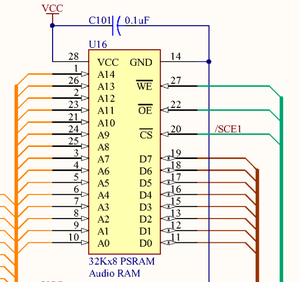
[[File:aram chip schematic.png|thumb|upper ARAM chip, straddling regions C4 and D4 of the [[jwdonal schematic]]]] | [[File:aram chip schematic.png|thumb|upper ARAM chip, straddling regions C4 and D4 of the [[jwdonal schematic]]]] | ||
There are two '''ARAM''' chips on the [[SNES Motherboard]], both connected to [[S-DSP]]. All accesses from the [[SPC700]] go through the S-DSP. ARAM is a total of 65,536 bytes (or 256 pages, or one bank) in size. | There are two '''ARAM''' chips on the [[SNES Motherboard]], both connected to [[S-DSP]]. All accesses from the [[SPC700]] go through the S-DSP. ARAM is a total of 65,536 bytes (or 256 pages, or one [[bank]]) in size. | ||
=== See Also === | === See Also === | ||
Revision as of 12:55, 16 December 2023

upper ARAM chip, straddling regions C4 and D4 of the jwdonal schematic
There are two ARAM chips on the SNES Motherboard, both connected to S-DSP. All accesses from the SPC700 go through the S-DSP. ARAM is a total of 65,536 bytes (or 256 pages, or one bank) in size.
See Also
References
- Page 2-22-3 of Book I of the official Super Nintendo development manual

