We've just updated MediaWiki and its underlying software. If anything doesn't look or work quite right, please mention it to us. --RanAS
VRAM: Difference between revisions
From SnesLab
(word addressed) |
(→Reference: added ref) |
||
| Line 13: | Line 13: | ||
* [[ARAM]] | * [[ARAM]] | ||
=== | === References === | ||
* [https://archive.org/details/SNESDevManual/book1/page/n195 Appendix A-1] of the official Super Nintendo development manual | * [https://archive.org/details/SNESDevManual/book1/page/n195 Appendix A-1] of the official Super Nintendo development manual | ||
* https://archive.org/details/SNESDevManual/book1/page/n97 | |||
[[Category:SNES Hardware]] | [[Category:SNES Hardware]] | ||
Revision as of 19:05, 11 August 2024

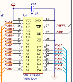
VRAM chip B in region B2 of the jwdonal schematic (directly north of chip A)
There are two VRAM chips on the SNES motherboard, both connected to S-PPU1. They are both SRAM and each 32K x 8 bit (32,768 bytes) in size, for a total of 65,536 bytes (one bank).
VRAM is word (not byte) addressed, with one chip holding the low bytes of the 16-bit words, the other chip holds the high bytes.
The two chips can be referred to as "A" and "B", after the lines of the VRAM Data Bus VDA0~7 and VDB0~7.
VRAM is not connected to Address Bus A, so the 5A22 must access it through I/O ports.
See Also
References
- Appendix A-1 of the official Super Nintendo development manual
- https://archive.org/details/SNESDevManual/book1/page/n97

