We've just updated MediaWiki and its underlying software. If anything doesn't look or work quite right, please mention it to us. --RanAS
Reset Traces: Difference between revisions
From SnesLab
(made schematic into thumbnail) |
(linkify jwdonal schematic) |
||
| (4 intermediate revisions by the same user not shown) | |||
| Line 1: | Line 1: | ||
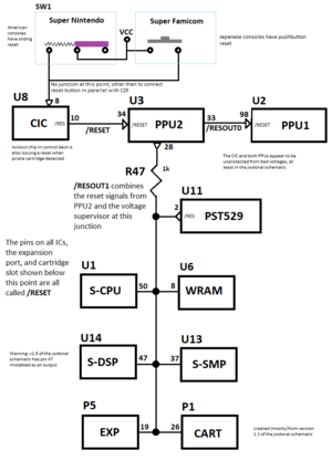
[[File:reset schematic v2.png|schematic of the various reset traces|thumb]] | |||
The SNES has a few traces used in system resetting: | The SNES has a few traces used in system resetting: | ||
/'''RESOUT0''' allows [[S-PPU2]] to reset [[S-PPU1]]. It is produced by pin 33 of PPU2 and goes into pin 98 (/RESET) of PPU1. It is not connected to anything else. | |||
/'''RESOUT0''' allows [[S-PPU2]] to reset [[S-PPU1]]. It is produced by pin 33 of PPU2 and goes into pin | |||
/'''RESOUT1''' is produced by pin 28 of [[S-PPU2]] and passes through R74 before combining with the [[voltage supervisor]] reset output. Then, RESOUT1 goes into these pins, all of which are labled /RESET: | /'''RESOUT1''' is produced by pin 28 of [[S-PPU2]] and passes through R74 before combining with the [[voltage supervisor]] reset output. Then, /RESOUT1 goes into these pins, all of which are labled /RESET: | ||
* pin 50 of the [[S-CPU]] | * pin 50 of the [[S-CPU]] | ||
| Line 14: | Line 14: | ||
* pin 47 of the [[S-DSP]] | * pin 47 of the [[S-DSP]] | ||
The trace (not pin) labeled /'''RESET''' on the jwdonal schematic is produced by pin 10 (P10) of the [[CIC]] and is what actually resets PPU2 (going into pin 34). | The trace (not pin) labeled /'''RESET''' on the [[jwdonal schematic]] is produced by pin 10 (P10) of the [[CIC]] and is what actually resets PPU2 (going into pin 34). | ||
=== See Also === | === See Also === | ||
Latest revision as of 07:10, 10 July 2023
The SNES has a few traces used in system resetting:
/RESOUT0 allows S-PPU2 to reset S-PPU1. It is produced by pin 33 of PPU2 and goes into pin 98 (/RESET) of PPU1. It is not connected to anything else.
/RESOUT1 is produced by pin 28 of S-PPU2 and passes through R74 before combining with the voltage supervisor reset output. Then, /RESOUT1 goes into these pins, all of which are labled /RESET:
- pin 50 of the S-CPU
- pin 8 of WRAM
- pin 26 of the Cartridge Slot
- pin 37 of the S-SMP
- pin 19 of the Expansion Port
- pin 47 of the S-DSP
The trace (not pin) labeled /RESET on the jwdonal schematic is produced by pin 10 (P10) of the CIC and is what actually resets PPU2 (going into pin 34).

