We've just updated MediaWiki and its underlying software. If anything doesn't look or work quite right, please mention it to us. --RanAS
Address Bus B: Difference between revisions
From SnesLab
(→Reference: hid archive URL) |
(pluralize) |
||
| Line 16: | Line 16: | ||
* [[Address Bus A]] | * [[Address Bus A]] | ||
=== | === References === | ||
# https://forums.nesdev.org/viewtopic.php?p=116505#p116505 | # https://forums.nesdev.org/viewtopic.php?p=116505#p116505 | ||
# Figure 2-22-1, "Super NES Functional Block Diagram" on [https://archive.org/details/SNESDevManual/book1/page/n98 page 2-22-2 of Book I] | # Figure 2-22-1, "Super NES Functional Block Diagram" on [https://archive.org/details/SNESDevManual/book1/page/n98 page 2-22-2 of Book I] | ||
Revision as of 04:23, 15 January 2024
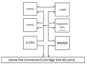
Address Bus B, also known as the SNES bus, is 8-bits wide on the SNES Motherboard. Its individual address lines are labeled PA0-PA7, which stands for "peripheral address," as in S-CPU peripherals (not SNES peripherals). It is connected to:
- pins 51-58 of the S-CPU
- pins 5-12 of S-PPU1
- pins 17-24 of S-PPU2
- pins 48-51 of S-SMP
- pins 43-50 and 53-54 of WRAM
- pins 28-30 and 59-61, 3 and 34 of the Cartridge Slot
- pins 1-8 of the Expansion Port
which is the exact same set of components that the CPU Data Bus is connected to. The SNES bus is drawn in purple in the colorized jwdonal schematic. Some people like to think of Address Bus B as being 16-bits wide, with the high byte being fixed to $21.[1]
See Also
References
- https://forums.nesdev.org/viewtopic.php?p=116505#p116505
- Figure 2-22-1, "Super NES Functional Block Diagram" on page 2-22-2 of Book I
- paragraph 3.2 on page 3-3-2 of Book I, lbid.


