We've just updated MediaWiki and its underlying software. If anything doesn't look or work quite right, please mention it to us. --RanAS
Address Bus A: Difference between revisions
From SnesLab
(linkify jwdonal schematic) |
(pin 33 of WRAM is GND and pin 32 is VCC) |
||
| (11 intermediate revisions by the same user not shown) | |||
| Line 2: | Line 2: | ||
It is connected to: | It is connected to: | ||
* pins 2-17 and 93-100 | * [[S-CPU]] pins 2-17 and 93-100 | ||
* [[WRAM]] pins 23-31 and pins 34-42 | |||
* [[Cartridge Slot]] pins 6-17 and 37-48 | |||
It is 24 bits wide because that is how big the SNES' address space is. It can address up to 16 megabytes, which is enough for most games, but some games use bank switching to address even more. | |||
[[File:Bus A.png|thumb]] | |||
=== See Also === | |||
* [[Address Bus B]] | |||
* [[CPU Data Bus]] | |||
=== Reference === | |||
# Figure 2-22-1, "Super NES Functional Block Diagram" on [https://archive.org/details/SNESDevManual/book1/page/n98 page 2-22-2 of Book I] | |||
[[Category:SNES Hardware]] | [[Category:SNES Hardware]] | ||
[[Category:Traces]] | [[Category:Traces]] | ||
[[Category:Buses]] | [[Category:Buses]] | ||
Latest revision as of 19:44, 18 August 2024
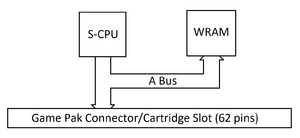
Address Bus A is a 24-bit bus on the SNES. It is drawn in orange in the colorized jwdonal schematic, and its individual address lines are labeled CA0-CA23.
It is connected to:
- S-CPU pins 2-17 and 93-100
- WRAM pins 23-31 and pins 34-42
- Cartridge Slot pins 6-17 and 37-48
It is 24 bits wide because that is how big the SNES' address space is. It can address up to 16 megabytes, which is enough for most games, but some games use bank switching to address even more.
See Also
Reference
- Figure 2-22-1, "Super NES Functional Block Diagram" on page 2-22-2 of Book I


